Hybrid Bonding Advances in Logic, Memory Adoption Slips to Late Decade
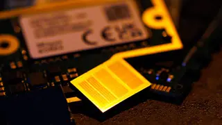
Hybrid bonding, which connects chip layers with copper instead of solder, is now used in volume for logic chips, with TSMC at a 6-micron pitch and plans for 4.5 microns by 2029. Intel and AMD have also adopted the technique. But a JEDEC change to HBM stack-height limits has postponed hybrid bonding in memory to HBM4E and HBM5, expected near the decade's end.
Hybrid bonding's two production methods carry distinct trade-offs. Wafer-to-wafer bonding aligns entire wafers at once, enabling the tightest pitches—researchers have demonstrated 200-nanometer spacing—but it pairs every die, including defective ones, wasting good silicon. Die-to-wafer bonding places individual pre-tested dies sequentially, which slows throughput but permits known-good-die selection and mixing of different die sizes and process nodes, making it essential for chiplet architectures and memory stacks.
The density advantage is substantial: face-to-face hybrid bonding achieves roughly 14,000 signals per square millimeter versus about 1,500 for face-to-back through-silicon-via stacking. Microbump technology has historically operated at 40-micron pitches, tightening toward 10 microns for recent memory, while hybrid bonding starts at 6 microns and has sub-micron pitches demonstrated in research. The JEDEC stack-height change allows HBM4 to remain on microbumps, deferring hybrid bonding's memory debut to HBM4E and HBM5.
This postponement could shape AI infrastructure economics for the next several years. Memory bandwidth is a critical bottleneck in AI accelerators, and hybrid bonding's delay may slow the pace of performance gains in high-end computing systems that rely on HBM. For consumers, the impact could appear indirectly through data-center costs and the pricing of AI services. The logic-side adoption by TSMC, Intel, and AMD may nonetheless accelerate competition in chip packaging, potentially driving down costs of advanced processors over time.