Industry giants join forces to enable single-pass chip printing with next-gen lithography
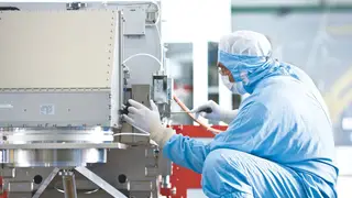
ASML, Intel, Samsung, and TSMC are jointly supporting the development of 6x12-inch photomasks for High-NA EUV lithography. The larger reticles would allow printing large chips in a single exposure, eliminating the need for stitching. The transition is expected to take several years despite the unified effort.
High-NA scanners employ asymmetric optics that shrink the printable area to a half-field, forcing manufacturers to combine two exposures for large processors. This joining process lowers output from roughly 175 to 125 wafers per hour and demands near-perfect overlay, as minor misalignments could create defects and erode yields on costly equipment. The proposed larger stencil would eliminate this two-step approach.
The alliance echoes earlier cooperative moves, like the abandoned 450-millimeter wafer initiative and the original push toward extreme ultraviolet tools. By pooling resources, these rivals acknowledge a shared bottleneck, yet adopting the new mask size remains a multi-year undertaking.
If successful, this transition could lower manufacturing costs and improve yields for large, complex chips, potentially leading to more powerful and affordable consumer devices like AI accelerators and high-end processors. However, the multi-year timeline means near-term benefits are limited. Consumers may see faster performance gains, while the semiconductor supply chain could become more consolidated around these key players, affecting pricing and technological advancement pace.