Extreme Ultraviolet Lithography Enables Ultra-Dense Chip Manufacturing
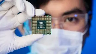
Extreme ultraviolet technology enables the creation of extraordinarily small circuit patterns that are orders of magnitude smaller than human hair. This manufacturing advancement underpins the development of modern high-performance processors used in contemporary computing devices. The technique allows for the integration of more transistors and functionality into increasingly compact chips.
Extreme ultraviolet lithography represents a significant refinement in semiconductor manufacturing technology. By utilizing shorter wavelengths of light, this approach enables fabrication processes to create vastly finer architectural details on silicon substrates compared to conventional methods. The resulting capability to pack computational components more densely directly supports the continued performance gains that end users experience in their devices.
This manufacturing process sits within the broader evolution of chip design, where successive generations have consistently worked to reduce the physical dimensions of electronic components while increasing their quantity and capability per unit area.
The advancement of chip manufacturing techniques affects multiple sectors of the technology industry and consumer base. Improved processor density could enable more powerful computing devices at comparable price points, potentially accelerating innovation in artificial intelligence, data processing, and mobile technologies. Manufacturers and technology companies may gain competitive advantages through production efficiency, while consumers could benefit from enhanced device performance and capabilities over time.