Large Language Models Transform Semiconductor Design Methodology
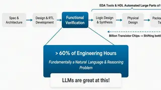
Large language models are revolutionizing chip design by enabling engineers to express design intent more intuitively beyond traditional RTL representations. The article explores how LLMs facilitate the shift toward higher-level abstractions in semiconductor development. This advancement comes as major technology companies increasingly pursue custom silicon to support next-generation AI infrastructure.
The semiconductor industry has experienced a fundamental shift in design bottlenecks over recent decades. Early limitations in synthesis and routing tools have been progressively overcome through EDA innovations, pushing engineering constraints toward the verification phase—a stage requiring exhaustive testing to ensure chips function correctly before expensive manufacturing. This evolution reflects how computational challenges migrate as tools advance, leaving new phases as the critical path in development cycles.
The acceleration of AI infrastructure demands is driving unprecedented interest in custom silicon development among major technology firms. However, creating specialized chips remains extraordinarily resource-intensive, typically requiring over 1,000 engineering months and teams exceeding 100 specialists across multiple design disciplines. Language models may help address this bottleneck by enabling designers to work at higher abstraction levels, potentially reducing development timelines and making chip design more accessible to organizations previously unable to undertake such projects.
If LLMs successfully streamline chip design, the implications could extend broadly across technology development. Organizations might gain ability to build custom processors more rapidly and cost-effectively, potentially democratizing AI infrastructure development beyond current industry leaders. Conversely, accelerating chip design could intensify competition in AI capabilities and computing power concentration. Society may benefit from faster innovation cycles, though questions remain about labor displacement for specialized engineers and whether efficiency gains translate to broader accessibility or remain concentrated among well-capitalized entities.