CFET Technology Path Forward: New Device Architectures Enable Sub-5-Track Standard Cells
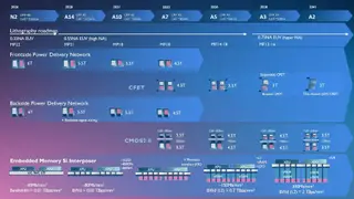
Part two of an analysis on complementary field-effect transistor advancement focuses on scalable standard cell designs and manufacturing integration strategies led by imec research. Novel split-gate and common-gate CFET architectures enable new SRAM configurations and improved routing efficiency in back-end manufacturing layers. These innovations support the industry transition toward sub-5-track standard cells expected at the A7 logic technology node and beyond.
Complementary field-effect transistors represent a significant departure from the dominant gate-all-around nanosheet design approach that currently powers advanced semiconductor nodes. By vertically stacking complementary transistor pairs, manufacturers can dramatically reduce the physical footprint required for standard cell designs. The research emerging from imec demonstrates that architectural innovations—particularly in how gate structures are configured and how signal routing occurs in manufacturing layers—are essential prerequisites for making this transition commercially viable at future technology generations.
CFET advancement could accelerate the timeline for continued semiconductor miniaturization, potentially sustaining Moore's Law economics for several additional technology generations. This may benefit computing performance and energy efficiency across consumer electronics, data centers, and AI systems. However, the transition requires substantial R&D investment and manufacturing process redesign, which could initially concentrate advanced chip production among better-resourced fabricators. Broader implications depend on whether CFET technologies become industry standards or remain specialized solutions for specific applications.