Catching Packaging Defects Before They Cause Expensive Failures
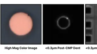
Advanced packaging builds value through many layers and steps, so a missed defect late in assembly can jeopardize an entire chiplet or memory stack. As package features shrink, inspection must find smaller flaws and handle more complex structures. The article discusses combining inspection and metrology methods to detect surface, sidewall, and subsurface issues such as particles, cracks, voids, and bump irregularities while measuring bump height and surface characteristics.
Advanced packaging creates value through successive layers, components, and process steps. By assembly, chiplets, high-bandwidth memory stacks, or hybrid-bonded devices already embody significant material and processing investment, so a defect missed late can threaten the whole assembly. Shrinking package features are also pushing packaging tolerances closer to those of front-end fabrication.
Process control must address surface, sidewall, and subsurface risks, including particles, cracks, embedded flaws, microbump irregularities, and bonding voids, while measuring bump height and surface profile. Sensitive two-dimensional imaging, infrared inspection beneath the surface, and three-dimensional measurement can be combined in one workflow, though throughput must remain high enough for volume production.
Better defect detection in advanced packaging may improve reliability of chips used in computing, communications, and data-intensive systems. Consumers and businesses could benefit from fewer premature failures and more dependable devices. Manufacturers may reduce wasted materials and costly scrap, potentially easing some supply constraints. Workers and engineers might see changing skill demands as inspection workflows integrate multiple techniques. These effects depend on cost, throughput, and adoption.