Intel's packaging roadmap: EMIB and Foveros evolve for broader chip scaling
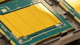
Intel began deploying EMIB and Foveros in 2017-2019, and these packaging methods now underpin many of its high-end client and data-center processors. The company's roadmap shows the two technologies becoming more capable for premium chips while also being adapted for cost-sensitive products, with EMIB and Foveros increasingly used together.
Intel's packaging efforts trace to 2017, when Kaby Lake-G CPUs and Stratix 10 FPGAs arrived, with EMIB reaching high-volume production. By 2020, Intel had outlined a multi-chiplet roadmap built around 2.5D EMIB and 3D Foveros. EMIB places small silicon bridges inside an organic substrate only where dense die-to-die links are needed, cutting silicon use and permitting looser bump pitches elsewhere. Early bridge pitch was 55 µm, later 45 µm, with roadmaps pointing toward 36 µm and eventually 25 µm.
Intel aims for system-in-packages up to 12 reticles using EMIB plus Foveros Direct 3D, potentially enabling AI accelerators with many bridges and over 24 HBM stacks.
Advances in EMIB and Foveros could influence how quickly faster, more capable processors reach data centers, PCs, and AI systems. Chip designers and manufacturers may gain flexibility to mix chiplets, potentially improving performance and cost trade-offs. Consumers and businesses could see benefits through more capable devices and services, though actual effects depend on yields, pricing, and adoption. The technology may also shape competition and supply-chain planning across the semiconductor industry.