Automated Via Insertion Targets Advanced-Node Interconnect Reliability
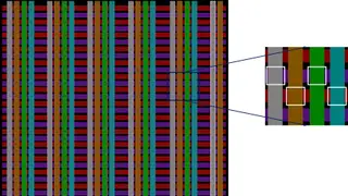
At advanced nodes below 5nm, interconnect wiring rather than gate delay increasingly limits power, performance, and area. Via resistance rises as dimensions shrink, worsening electromigration and IR-drop issues that design teams often handle late in signoff. The article discusses automated via insertion and moving signoff-aware optimization earlier into implementation to improve reliability and avoid schedule delays.
At nodes below 5nm, wiring delays and power delivery constraints increasingly outweigh transistor switching speed as the main design limit. Vias, the vertical links between metal layers, become especially vulnerable because their resistance climbs sharply as they shrink, while current density rises.
That combination worsens electromigration and IR drop, which can slow gates or cause timing failures. Manual redundant-via insertion once helped lower current density and resistance, but dense layouts and complex foundry rules make it impractical. Automated insertion and earlier signoff-aware optimization aim to address these reliability risks without late ECOs.
Better via reliability at advanced nodes could affect chip designers, foundries, and ultimately people who depend on computing, communications, vehicles, and data centers. If signoff-aware automation reduces late fixes and improves long-term dependability, electronics may become more reliable and product schedules more predictable. Those gains could be uneven, since advanced-node manufacturing remains concentrated and costly, so availability and pricing of affected devices may vary.