Apple's M6 Chip Leverages TSMC's 2nm Process for Density and Performance Gains
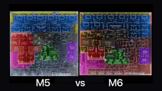
Apple's new M6 processor represents the first consumer-grade implementation of TSMC's advanced 2nm manufacturing process, allowing the company to increase core counts and cache while actually reducing the chip's overall size compared to the M5. The 2nm process introduces GAAFET transistor technology that reduces power leakage and enables higher clock speeds by surrounding gate material on all four sides. Technical analyses reveal significant architectural improvements, though some observers note that bandwidth limitations may constrain the chip's full potential despite its manufacturing advantages.
Apple's M6 processor marks a watershed moment in consumer chip manufacturing by being among the first mass-market implementations of TSMC's 2nm fabrication technology. The advancement permits Apple to pack more computational capability into a physically smaller footprint—the M6 measures approximately 142 square millimeters compared to the M5's 157 square millimeters—while simultaneously expanding core counts and memory capacity. This density improvement stems from the introduction of GAAFET transistor architecture, which surrounds gate material on all sides rather than three, thereby reducing power consumption and enabling higher operating frequencies.
The M6 introduces a novel three-tier CPU hierarchy comprising 2 super cores, 4 performance cores, and 6 efficiency cores—a departure from Apple's previous dual-core strategy. This architectural reorganization effectively trades some peak single-thread capability for substantially improved multi-threaded performance without meaningfully increasing die size, suggesting Apple prioritized balanced computing workloads over raw speed. Technical analysts have noted that despite these manufacturing and architectural advances, memory bandwidth constraints may ultimately limit the chip's real-world performance ceiling.
The M6's 2nm process represents a meaningful inflection point for device performance and energy efficiency across consumer computing. Professionals relying on multi-threaded workloads—video editors, software developers, data analysts—may experience tangible productivity gains from the expanded core configuration. Broader industry implications could include accelerated adoption timelines for advanced manufacturing processes and potential cost-to-performance adjustments across the computing market. However, whether bandwidth limitations prove practically consequential for typical users remains an open question requiring extended real-world deployment data.