Electrical Signals Become Key to Advanced Packaging Control
As transistor scaling slows, packaging advances are becoming central for AI, high-performance computing, smartphones, automotive electronics, and networking. While most process-control attention goes to visible defects, hidden electrical conditions can reduce downstream yield, reliability, and manufacturing consistency. Residual charge control is especially important as new package designs incorporate more moisture-absorbing films and materials.
Advanced packaging now matters alongside transistor miniaturization for AI, high-performance computing, smartphones, cars, and networking, because these systems need more bandwidth, better energy use, and added functions in tighter spaces. Much process-control attention goes to visible defects, yet electrical conditions can quietly lower later yield, reliability, and consistency, and ordinary inspection may miss them.
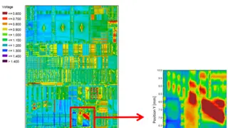
Residual charge is a growing concern. New package designs use more moisture-absorbing films and materials alongside insulating layers and substrates, requiring stricter environmental management. In dry conditions, static and leftover charge can accumulate, while plasma, deposition, cleaning, surface prep, and bonding steps can create localized charge across wafers and panels. Mapping can reveal non-uniformities and hotspots.
Better electrical process control in chip packaging could affect consumers, automakers, device makers, and manufacturers. If residual charge issues are reduced, electronics may become more reliable and production more consistent, potentially improving availability and performance of AI systems, phones, vehicles, and networks. If not addressed, hidden electrical problems may contribute to yield losses and reliability concerns, affecting costs and access to advanced electronics.